| Author |
All about display drivers sony ericsson mobile phone |
brazzuka's
Joined: Nov 14, 2007
Posts: > 500
From: South World-Antartida-Sweden
PM, WWW
|
For all developers modders and users Here you can find Modded Dispdrivers for Sony Ericsson mobile phone
| |
|
brazzuka's
Joined: Nov 14, 2007
Posts: > 500
From: South World-Antartida-Sweden
PM, WWW
|
Learn About LCD TV and TFT LCD Displays
History of TFT LCD
Liquid crystal was discovered by the Austrian botanist Fredreich Rheinizer in 1888. "Liquid crystal" is neither solid nor liquid (an example is soapy water).
In the mid-1960s, scientists showed that liquid crystals when stimulated by an external electrical charge could change the properties of light passing through the crystals.
The early prototypes (late 1960s) were too unstable for mass production. But all of that changed when a British researcher proposed a stable, liquid crystal material (biphenyl).
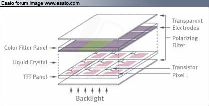
Today's color LCD TVs and LCD Monitors have a sandwich-like structure (see figure below).
What is TFT LCD?
TFT LCD (Thin Film Transistor Liquid Crystal Display) has a sandwich-like structure with liquid crystal filled between two glass plates.
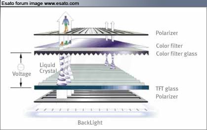
TFT Glass has as many TFTs as the number of pixels displayed, while a Color Filter Glass has color filter which generates color. Liquid crystals move according to the difference in voltage between the Color Filter Glass and the TFT Glass. The amount of light supplied by Back Light is determined by the amount of movement of the liquid crystals in such a way as to generate color.
TFT LCD - Electronic Aspects of LCD TVs and LCD Monitors
Electronic Aspects of AMLCDs
The most common liquid-crystal displays (LCDs) in use today rely on picture elements, or pixels, formed by liquid-crystal (LC) cells that change the polarization direction of light passing through them in response to an electrical voltage.
As the polarization direction changes, more or less of the light is able to pass through a polarizing layer on the face of the display. Change the voltage, and the amount of light is changed.
There are two ways to produce a liquid-crystal image with such cells: the segment driving method and the matrix driving method.
The segment driving method displays characters and pictures with cells defined by patterned electrodes.
The matrix driving method displays characters and pictures in sets of dots.
Direct vs. multiplex driving of LCD TVs.
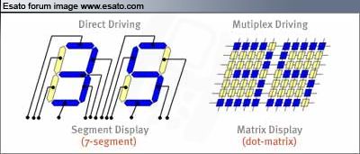
The segment drive method is used for simple displays, such as those in calculators, while the dot-matrix drive method is used for high-resolution displays, such as those in portable computers and TFT monitors.
Two types of drive method are used for matrix displays. In the static, or direct, drive method, each pixel is individually wired to a driver. This is a simple driving method, but, as the number of pixels is increased, the wiring becomes very complex. An alternative method is the multiplex drive method, in which the pixels are arranged and wired in a matrix format.
To drive the pixels of a dot-matrix LCD, a voltage can be applied at the intersections of specific vertical signal electrodes and specific horizontal scanning electrodes. This method involves driving several pixels at the same time by time-division in a pulse drive. Therefore, it is also called a multiplex, or dynamic, drive method.
Passive and Active Matrix LCDs
There are two types of dot-matrix LCDs.
Passive-matrix vs. active-matrix driving of LCD Monitors.
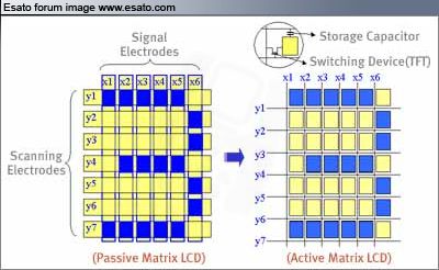
In passive-matrix LCDs (PMLCDs) there are no switching devices, and each pixel is addressed for more than one frame time. The effective voltage applied to the LC must average the signal voltage pulses over several frame times, which results in a slow response time of greater than 150 msec and a reduction of the maximum contrast ratio. The addressing of a PMLCD also produces a kind of crosstalk that produces blurred images because non-selected pixels are driven through a secondary signal-voltage path. In active-matrix LCDs (AMLCDs), on the other hand, a switching device and a storage capacitor are integrated at the each cross point of the electrodes.
The active addressing removes the multiplexing limitations by incorporating an active switching element. In contrast to passive-matrix LCDs, AMLCDs have no inherent limitation in the number of scan lines, and they present fewer cross-talk issues. There are many kinds of AMLCD. For their integrated switching devices most use transistors made of deposited thin films, which are therefore called thin-film transistors (TFTs).
The most common semiconducting layer is made of amorphous silicon (a-Si).
a-Si TFTs are amenable to large-area fabrication using glass substrates in a low-temperature (300�C to 400�C) process.
An alternative TFT technology, polycrystalline silicon - or polysilicon or p-Si-is costly to produce and especially difficult to fabricate when manufacturing large-area displays.
Nearly all TFT LCDs are made from a-Si because of the technology's economy and maturity, but the electron mobility of a p-Si TFT is one or two orders of magnitude greater than that of an a-Si TFT.
This makes the p-Si TFT a good candidate for an TFT array containing integrated drivers, which is likely to be an attractive choice for small, high definition displays such as view finders and projection displays.
Structure of Color TFT LCD TVs and LCD Monitors
A TFT LCD module consists of a TFT panel, driving-circuit unit, backlight system, and assembly unit.
Structure of a color TFT LCD Panel:
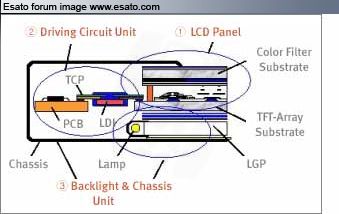
1. LCD Panel
- TFT-Array Substrate
- Color Filter Substrate
2. Driving Circuit Unit
- LCD Driver IC (LDI) Chips
- Multi-layer PCBs
- Driving Circuits
3. Backlight & Chassis Unit
- Backlight Unit
- Chassis Assembly
It is commonly used to display characters and graphic images when connected a host system.
The TFT LCD panel consists of a TFT-array substrate and a color-filter substrate.
The vertical structure of a color TFT LCD panel.
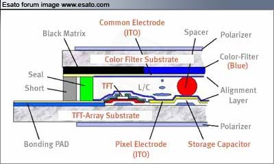
The TFT-array substrate contains the TFTs, storage capacitors, pixel electrodes, and interconnect wiring. The color filter contains the black matrix and resin film containing three primary-color - red, green, and blue - dyes or pigments. The two glass substrates are assembled with a sealant, the gap between them is maintained by spacers, and LC material is injected into the gap between the substrates. Two sheets of polarizer film are attached to the outer faces of the sandwich formed by the glass substrates. A set of bonding pads are fabricated on each end of the gate and data-signal bus-lines to attach LCD Driver IC (LDI) chips
Driving Circuit Unit
Driving an a-Si TFT LCD requires a driving circuit unit consisting of a set of LCD driving IC (LDI) chips and printed-circuit-boards (PCBs).
The assembly of LCD driving circuits.
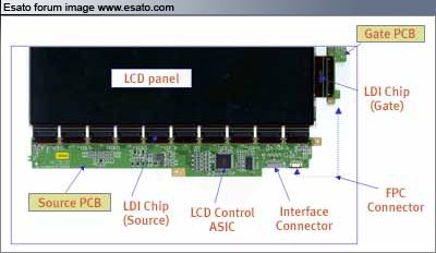
A block diagram showing the driving of an LCD panel.
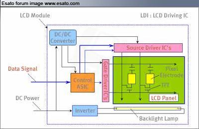
To reduce the footprint of the LCD module, the drive circuit unit can be placed on the backside of the LCD module by using bent Tape Carrier Packages (TCPs) and a tapered light-guide panel (LGP).
How TFT LCD Pixels Work
A TFT LCD panel contains a specific number of unit pixels often called subpixels.
Each unit pixel has a TFT, a pixel electrode (IT0), and a storage capacitor (Cs).
For example, an SVGA color TFT LCD panel has total of 800x3x600, or 1,440,000, unit pixels.
Each unit pixel is connected to one of the gate bus-lines and one of the data bus-lines in a 3mxn matrix format. The matrix is 2400x600 for SVGA.
Structure of a color TFT LCD panel.
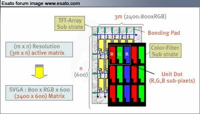
Because each unit pixel is connected through the matrix, each is individually addressable from the bonding pads at the ends of the rows and columns.
The performance of the TFT LCD is related to the design parameters of the unit pixel, i.e., the channel width W and the channel length L of the TFT, the overlap between TFT electrodes, the sizes of the storage capacitor and pixel electrode, and the space between these elements.
The design parameters associated with the black matrix, the bus-lines, and the routing of the bus lines also set very important performance limits on the LCD.
In a TFT LCD's unit pixel, the liquid crystal layer on the ITO pixel electrode forms a capacitor whose counter electrode is the common electrode on the color-filter substrate.
Vertical structure of a unit pixel and its equivalent circuit
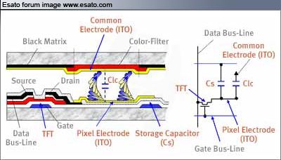
A storage capacitor (Cs) and liquid-crystal capacitor (CLC) are connected as a load on the TFT.
Applying a positive pulse of about 20V peak-to-peak to a gate electrode through a gate bus-line turns the TFT on. Clc and Cs are charged and the voltage level on the pixel electrode rises to the signal voltage level (+8 V) applied to the data bus-line.
The voltage on the pixel electrode is subjected to a level shift of DV resulting from a parasitic capacitance between the gate and drain electrodes when the gate voltage turns from the ON to OFF state. After the level shift, this charged state can be maintained as the gate voltage goes to -5 V, at which time the TFT turns off. The main function of the Cs is to maintain the voltage on the pixel electrode until the next signal voltage is applied.
Liquid crystal must be driven with an alternating current to prevent any deterioration of image quality resulting from dc stress.
This is usually implemented with a frame-reversal drive method, in which the voltage applied to each pixel varies from frame to frame. If the LC voltage changes unevenly between frames, the result would be a 30-Hz flicker.
(One frame period is normally 1/60 of a second.) Other drive methods are available that prevent this flicker problem.
Polarity-inversion driving methods.
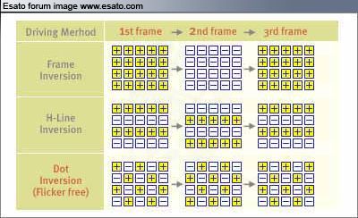
In an active-matrix panel, the gate and source electrodes are used on a shared basis, but each unit pixel is individually addressable by selecting the appropriate two contact pads at the ends of the rows and columns.
Active addressing of a 3x3 matrix
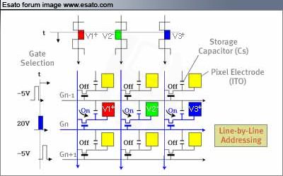
By scanning the gate bus-lines sequentially, and by applying signal voltages to all source bus-lines in a specified sequence, we can address all pixels. One result of all this is that the addressing of an AMLCD is done line by line.
Virtually all AMLCDs are designed to produce gray levels - intermediate brightness levels between the brightest white and the darkest black a unit pixel can generate. There can be either a discrete numbers of levels - such as 8, 16, 64, or 256 - or a continuous gradation of levels, depending on the LDI.
The optical transmittance of a TN-mode LC changes continuously as a function of the applied voltage.
An analog LDI is capable of producing a continuous voltage signal so that a continuous range of gray levels can be displayed.
The digital LDI produces discrete voltage amplitudes, which permits on a discrete numbers of shades to be displayed. The number of gray levels is determined by the number of data bits produced by the digital driver.
Generating Colors
The color filter of a TFT LCD TV consists of three primary colors - red (R), green (G), and blue (B) - which are included on the color-filter substrate.
How an LCD Panel produces colors.
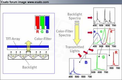
The elements of this color filter line up one-to-one with the unit pixels on the TFT-array substrate.
Each pixel in a color LCD is subdivided into three subpixels, where one set of RGB subpixels is equal to one pixel.
(Each subpixel consists of what we've been calling a unit pixel up to this point.)
Because the subpixels are too small to distinguish independently, the RGB elements appear to the human eye as a mixture of the three colors.
Any color, with some qualifications, can be produced by mixing these three primary colors.
The total number of display colors using an n-bit LDI is given by 23n, because each subpixel can generate 2n different transmittance levels.
TFT LCD - Fabricating TFT LCD
Fabricating Color TFT LCD Displays
The pressure to reduce the manufacturing cost of TFT LCD displays is as constant and intense as it is in the semiconductor industry. To increase productivity, IC makers continuously reduce the sizes of c-Si chips and transistors in order to increase the number of chips per wafer.
IC makers increase productivity by continuously reducing chip size and
increasing wafer size to increase the number of chips per wafer.
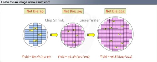
But this strategy doesn't work for LCDs because the panel sizes users demand most get steadily larger, not smaller.
Still, by increasing the number of panels produced on a single substrate, the cost of TFT-array processes can be reduced.
The IC makers' size-reduction strategy doesn't work for direct-view LCDs, but LCD manufacturers can still reduce the cost of TFT-array processes by increasing the number of panels produced on a single substrate.

This process requires that the size of the glass substrate be steadily increased so that the number of LCD panels fabricated upon it can increase.
For more panels to be put on a glass substrate, the substrate size must be steadily increased - which requires the continual design and construction of new generations of process equipment.
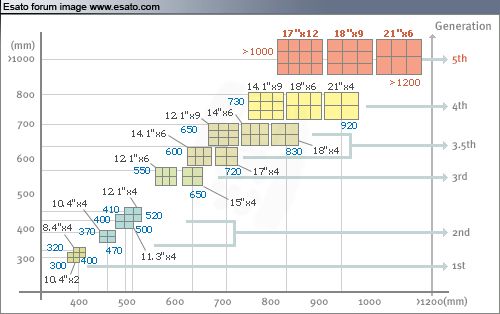
New generations of process equipment must be continually designed and built to achieve these increases.
The fabrication processes this equipment must implement will be described below.
We can assume that the display being fabricated is a color TFT LCD that uses an inverse-staggered-type a-Si TFT as the active-matrix switching element.
Fabricating the TFT array
The manufacturing process used to fabricate an a-Si TFT array is very similar to those used to fabricate c-Si semiconductor devices. The various steps, including cleaning, deposition of thin films, photolithography, and wet and dry etching of the thin films - are alsso very similar. The difference between the a-Si TFT process and the c-Si semiconductor process is that a semiconductor layer is deposited onto a glass substrate in the a-Si TFT process, while Si wafers are used as the substrate in the c-Si semiconductor process. Today, critical issues in the processing of TFT arrays include the development of a low-resistance gate-bus line, uniform and fine etching, and improved lithographic accuracy.
TFT-array technologies are aimed at achieving high precision, large aperture ratio, and low power consumption, in addition to large screen size.
AMLCD manufacturers are also competing to minimize the number of array processes by reducing the number of photo masks and simplifying the thin-film-formation and etching processes.
In the bottom-gate TFT-array fabrication process, the first layer consists of the gate electrodes and gate bus-lines, which can have one or two metal layers.
Some storage capacitors can be constructed by using a part of the gate electrode as an electrode of the storage capacitor - which is called the Cs-on-gate method - while other capacitors are constructed independent of a gate bus-line.
If the independent Cs lines are constructed simultaneously with the gate bus-lines using the same metal layer, there is no difference in the fabrication process between the Cs-on-gate method and the independent Cs bus-line method.
The processing of an a-Si TFT array is complex.
This flowchart outlines the processes for making an a-Si TFT array using a bottom-gate TFT structure and an independent storage capacitor.
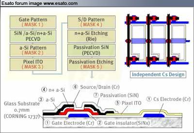
After constructing gate and storage-capacitor electrodes with 2000-3000A of a metal such as aluminum, chromium, tantalum, or tungsten, a triple layer of silicon nitride and amorphous silicon is deposited by using plasma-enhanced chemical-vapor deposition (PECVD).
In the etch-back type of TFT structure, the triple layer consists of 4000A of SiNx, 2000A of a-Si, and 500 A OF n+a-si, which is deposited over the gate electrode in a continuous process, i.e., a process without a vacuum break.
For the etch-stopper type of TFT structure, 4000A of SiNx, 500A OF a-Si, and 2000A of n+a-si are deposited.
Let us look at the etch-back TFT fabrication process in more detail.
TFT Fabrication
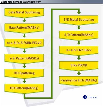
After defining the a-Si area by using photolithography and plasma dry etching, an ITO layer is deposited with a thickness of about 500A via sputtering.
Then, the pixel electrodes are patterned. About 2000A of metal is sputter deposited, while data bus-lines and TFT electrodes are patterned by photolithography.
Then the ohmic contact layer (n+a-Si) at the channel region is etched by dry etching using the source and drain electrodes as an etch-protect mask.
Finally, a protective 2500A SiNx layer is deposited by PECVD and contact windows are opened.
The etch-stopper TFT structure requires one more process step - a chemical vapor deposition (CVD) - than does the etch-back TFT structure.
For etch-stopper TFT fabrication, a n+a-Si layer is deposited separately after the top insulator of triple-layer (SiNx/a-Si/SiNx) is patterned.
The a-Si area is patterned and the n+a-Si layer at the top of etch-stopper is removed. The source and drain electrodes are formed using about 2000A of metal; then, about 500A of ITO is sputter deposited, and pixel electrodes are patterned.
A SiNx protective layer is then deposited by PECVD and, finally, the contact windows are opened.
Fabricating Color Filters
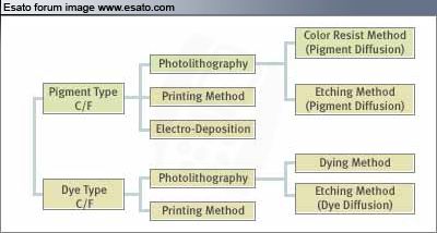
Color filters (CFs) can be made with either dyes or pigments, utilizing coloring method such as dyeing, diffusion, electro-deposition, and printing.
Color filters (CFs) can be made with either dyes or pigments, and can be
further divided by coloring method.
There are several fairly common color-element configurations for LCDs.
Stripe is the most popular, followed by mosaic and delta.
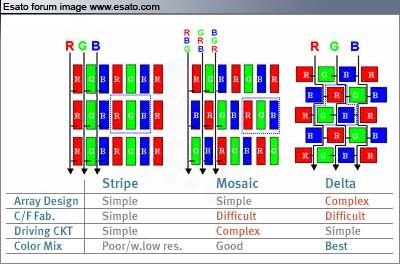
Among the many combinations of configuration and types of CF fabrication methods, the color-resist method with stripe-type RGB arrangement is currently the most popular.
Between the blocks of color in the CF is a black matrix (BM) made of an opaque metal, such as chromium, which shields the a-Si TFTs from stray light and prevents light leakage between pixels.
A double layer of Cr and CrOx is used to minimize reflection from the BM.
The sputter-deposited BM film is patterned using photolithography.
For reduced cost and reflectivity, black resin made by diffusing C and Ti in photo resist - can be used as a BM material.
In the color-resist method, the primary color-filter patterns are formed by using a photolithography technique.
The color-resist is negative and made by diffusing pigment in a UV-curing resin, such as an acryl-epoxy resin, and by dissolving the resin in a solvent.
A red colored resist is spin-coated onto a glass substrate on which a BM has previously been formed.
The red pattern is then formed by exposing the red resist through a mask and developing it.
The process is repeated using the same mask with a shifted mask-align technique for green- and blue-colored resins.
A protective film is then applied, and 1500A of ITO for the TFT array's common electrode is sputter-deposited to finish the color filter.
Liquid-crystal Cell Process
The TFT-array and color-filter substrates are made into an LCD panel by assembling the two substrates together with a sealant, while the cell gap is maintained by spacers.
The TFT-array and color-filter substrates are made into an LCD panel by
assembling them with a sealant.
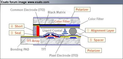
The assembly is begun by printing a polyimide alignment film on a cleaned TFT-array, and then rubbing the surface of the film with a piece of cloth wound on a roller, which orients the polyimide molecules in one direction.
Similarly, alignment film is applied to the color-filter substrate, and this substrate is also rubbed.
After the rubbing process, a sealant is applied to the periphery of the TFT-array substrate. To form electrical connections from the common electrodes on the color-filter substrate to the TFT array, the TFT-array substrate is coated with a conducting paste around the periphery.
At the same time, spacers to control the cell gap are sprayed onto the color-filter substrate. (In some cases, spacers are sprayed on to the TFT-array substrate, and a sealant is applied to the color-filter substrate.)
The two substrates are then assembled after the sealant is pre-hardened.
The sealant is then hardened completely with heat and pressure.
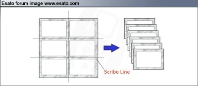
Then, the assembled substrates are scribed using a diamond wheel and separated into individual cells, and the empty cells are filled with liquid crystal material by vacuum injection.
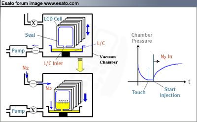
Finally, a sealing agent is used to seal the cell, and the polarizers are applied to both cell surfaces after a visual function test.
Assembling LCD Modules
Although critical for producing panels with the desired characteristics and price, the details of the manufacturing process for AMLCD panels are often of less immediate interest to the OEM purchasers of displays than are the details of the module assembly process.
This is so because it is the physical and electrical characteristics of the module that OEMs must deal with when integrating the display into products for end users.
The process flow for assembling a module using the tape-automated-bonding (TAB) method is conceptually straightforward, but it's not simple.
The process for assembling LCD modules(flow chart).
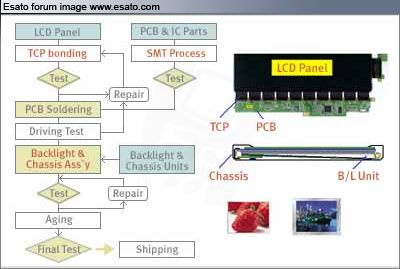
The first decision to make is whether you want to use TAB at all, or whether you would prefer the other basic way of applying the LDI chips needed to drive the TFT panel.
In the TAB method, the LDI chip is attached to a tape-carrier package (TCP), and the TCPs are then connected to the TFT-array substrate.
The structure of the tape-carrier package used in TAB.
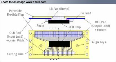
Anisotropic conducting film (ACF) is applied to the contact pads, where the stripe-shaped contact leads are formed as a group. The TCPs are then aligned and subjected to pressure-bonding.
The drive-circuit components, such as the timing controller, EMI filters, op amps, chip capacitors, and resistors, are mounted onto a multi-layered PCB using a surface-mount technology (SMT).
A soldering method is usually employed to connect the gate and control PCBs to the other end of the TCP leads, but in some cases ACF bonding can be used instead.
Mounting a TAB using a TCP and ACF.
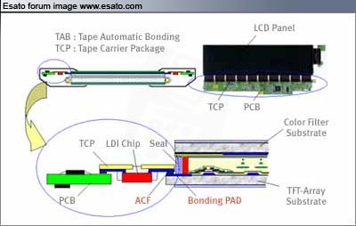
Sometimes, to minimize bezel size, the drive-circuit unit is set to the back side of the LCD module by using bent TCPs.
Alternatively, one can use the chip-on-glass (COG) method, in which LDI chips are mounted directly on the TFT-array substrate.
Chip-on-glass vs. tape-automated bonding.
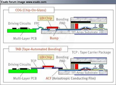
The choice of COG or TAB is determined by the peripheral area available and the limitations on bezel size for the display.
After testing the electrical functions, only the good LCD panels are subjected to the final assembly process, in which a backlight unit and a metal bezel are attached to compete the LCD module.
TFT Device Design
There are many structures for thin-film transistors (TFTs), with the first major distinction among them being planar CMOS structures vs. staggered amorphous-silicon (a-Si) structures.
Structure of TFT electrodes
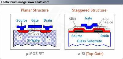
The a-Si TFTs are further divided into staggered and inverse-staggered types.
Structural difference between top- and bottom-gate TFTs
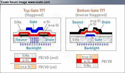
In the inverse-staggered type, the ohmic layer (n+ a-Si) in the channel region can either be etched directly (the etch-back method) or etched by forming a protective film on the a-Si thin film (the etch-stopper method).
Each method has its own set of advantages and disadvantages. The inverse-staggered structure offers a relatively simple fabrication process and an electron mobility that is about 30 percent larger than that of the staggered type. These advantages have resulted in the bottom-gate TFT structure becoming more widely adopted in TFT-LCD design, despite the fact that it's technically an upside-down structure.
Because a-Si has photoelectric characteristics, the a-Si TFT must be shielded from incident light .The a-Si layer must also be as thin as possible to minimize the generation of photo-induced current, which can cause the TFT to malfunction.
Reduction of photo-induced leakage current in a TFT
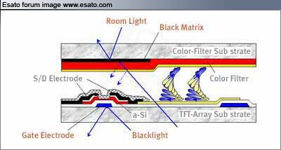
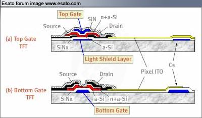
In the top-gate structure, a light-shield layer must first be formed at the region of the TFT channel The formation of this light shield may cause an extra process step. In bottom-gate TFTs, on the other hand, a gate electrode is first formed at the TFT channel region, where it also serves as a light-shield layer.
Light-shielding structures in a TFT-Array
Design Parameters for TFT Arrays
The operational characteristics of a TFT are determined by the sizes of its electrodes, the W/L ratio, and the overlap between the gate electrode and the source-drain .
Design of an a-Si TFT
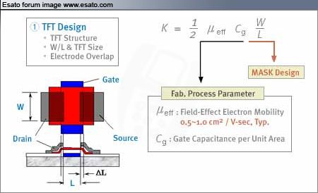
The parasitic capacitances resulting from the overlap of electrodes can not be avoided in staggered TFT structures, but the parasitic effects must be minimized to maximize the LCD's performance.
To reduce the overlap between the electrodes, a self-align process is often implemented .
Minimizing parasitic capacitance in TFTs
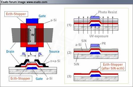
It turns out that the characteristics of the a-Si TFTs used in AMLCDs are very similar to the characteristics of the MOSFETs in semiconductor devices.
I-V Characteristics of an a-Si TFT and its operating points
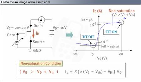
When a TFT panel is operated under real-world conditions, the gate voltage is set at either 20 V for switch-on, or at -5 V for switch-off. Under these operating conditions, the a-Si TFT is a good switching device with an on/off current ratio larger than 106.
The performance of the TFT also depends on fabrication process parameters, such as electron mobility and thickness of the gate insulators. If we wish to increase the current gain of the TFT for better pixel-switching performance, and the process parameters are fixed, the only thing we can do is increase the W/L ratio. But doing this is not without a significant trade-off: The larger W/L results in a lower aperture ratio - less of the pixel's area is transparent to light when the pixel is ON - so the display's brightness and contrast are reduced.
Storage Capacitor Design
To maintain a constant voltage on a charged pixel over the entire frame cycle, a storage capacitor (Cs) is fabricated at each pixel. A large Cs can improve the voltage holding ratio of the pixel and reduce the kickback voltage, with resulting improvements in contrast and flicker, but a large Cs results in a lower aperture ratio and higher TFT load.
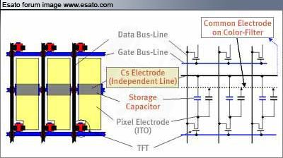
The storage capacitor can be formed by using either an independent storage-capacitor electrode or part of the gate bus-line as a storage-capacitor electrode (Cs-on-gate method)
Example of an independent-Cs design and equivalent circuit
Example of a Cs-on-gate design and equivalent circuit
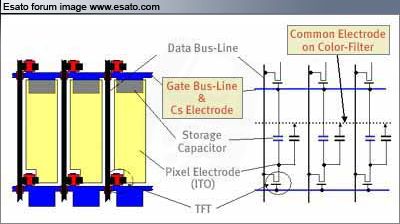
The advantages of the Cs-on-gate method are that it eliminates the need for modification in the fabrication process; it minimizes the number of processes; and it produces a larger aperture ratio than does the independent Cs method. But few things are free in TFT-LCD design. The trade-off with the Cs-on-gate method is an increase in the RC time constant of the gate bus-line, which reduces the TFT switching performance.
This RC delay problem can have serious effects on the appearance of the display.
RC delay of a gate signal and its effect on a black display

The solution lies in fabricating the gate bus-line with a low-resistance material such as aluminum (Al).
Signal Bus-line Design
The requirement that the gate bus-line must have a small RC time delay is particularly important for larger and higher-resolution LCDs. If the widths of the signal bus-lines are increased to reduce resistance, the aperture ratio of the pixels is reduced, so the preferred approach is to use a low-resistance material for the bus-lines. For this, Al offers advantage over other metals, such as Cr, W, and Ta.
But, in the bottom-gate TFT process, the gate electrodes are first fabricated on the glass substrate and then subjected to high-temperature processes and various chemical etches. So, to use Al as a gate-electrode material, the Al gate electrodes must be protected from damage produced by hillock formation.
Design of low-resistance aluminum gate bus-line
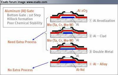
A thin film of an aluminum oxide (Al2O3), formed by anodic oxidation of the Al surface at room temperature, can protect the Al electrodes from the problems associated with hillock formation. Double-metal or clad structures over the Al electrodes - using a relatively stable material such as Cr, Ta, or W - can also be used to protect the Al electrodes. The trade-off is that these approaches require an additional process. Recently, Al alloy (such as Al-Nd), which can suppress hillock formation, has been used as a gate-electrode material to eliminate the additional process.
Aperture Ratio
As implied previously, another important design consideration is maximizing the aperture ratio of the pixel. In the unit cell, TFT electrodes, storage-capacitor electrodes, signal bus-lines, and the black-matrix material constitute opaque areas.
Opaque areas and aperture ratio of a pixel
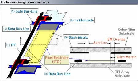
The combined areas of these elements, along with the area of the pixel aperture through which light can pass, determine the aperture ratio of the pixel. The aperture ratio is given by the area of the pixel aperture divided by the total pixel area (aperture area plus the area of the opaque elements). To increase the aperture ratio as much as possible, the size of the opaque elements must be made as small as possible, while maintaining a design that maximizes the size of the pixel-electrode area.
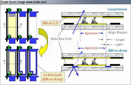
Unfortunately, one can only go so far in reducing the opaque areas before degrading image quality and yield. As shown in Fig. 12, the light-shield area on the color-filter substrate must be extended to block the light leaking through the gap between the data-line and the pixel ITO. To do this in conventional TFT-LCD cell structures, while simultaneously providing an adequate plate-alignment margin, significantly reduces the aperture.
But far higher aperture ratios can be achieved by switching from a conventional structure to the BM-on-Array structure, regardless of the accuracy of the plate alignment. The aperture ratio of this cell structure is not determined by the BM opening at the color filter substrate, but by the BM-on-Array, which can be formed with a very high positioning accuracy.
Improvement of aperture ratio using a black-matrix-on-TFT-array
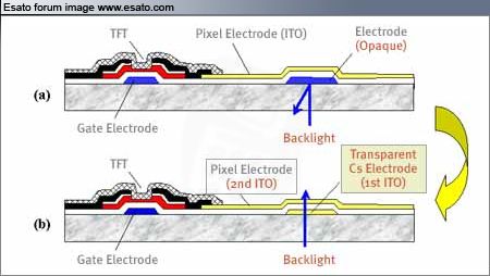
In an independent-Cs-electrode design, the aperture ratio can be increased if the storage-capacitor electrode is fabricated using ITO.
Improvement of aperture ratio using an ITO layer as a Cs electrode
Design for Redundancy
Even when the greatest care is taken and sophisticated quality-management procedures are applied, it is not possible to make the TFT-array fabrication process so perfect that it produces only completely defect-free arrays.
Possible line and pixel defects on a TFT array
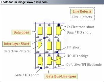
To improve the production yield in the fabrication process, redundancy design, repairable design, and fault-tolerant designs are often used. Dual-bus-line design or double-metal structure can help recover from problems of line breakage. Dummy-repair-line design can save the defective panel from data-bus-line open failures. While these redundant-design techniques can effectively improve fabrication yield, in some cases they can also reduce the aperture ratio.
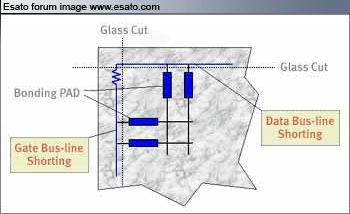
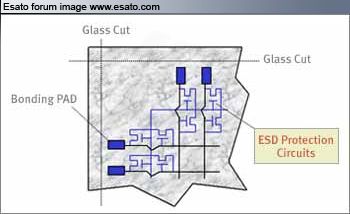
The TFT-array must be protected from electrostatic discharge (ESD), which can be generated in the fabrication processes such as during the rubbing of the alignment layer and spin-drying. Design approaches for protecting the TFT-array against ESD include bus-line shorting and ESD protection circuits.
ESD protection using a bus-line shorting method
ESD protection using protection circuits
TFT LCD - Precaution and Failure
Temperature / Humidity
It is recommended to use the product at room temperature and humidity in order to maintain it's optimum performance.
1. Product lifetime can be shortened when it is used under conditions of high temperature and humidity.
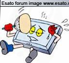
2. When it is used at low temperature of 10�C or lower, response time and brightness are affected in such a way that the proper display may not be obtained.

3. When exposed to drastic fluctuation of temperature (hot to cold or cold to hot), the product may be affected; specifically, drastic temperature fluctuation from cold to hot, produces dew on the surface which may affect the operation of the polarizer and product.
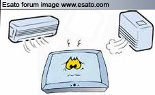
Environmental Consideration
It is recommended to use the product in a clean place and to exercise caution to ensure it is not affected by dust or liquids, etc.
1. If used in dusty place, dust may cause an electrical short inside the product resulting in malfunction

2. If the product is contaminated by humid or liquid substance, polarizer may be discolored. If the liquid enters may enter the product to cause electrical failure or corrosion which, in turn, may lead to malfunction
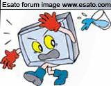
Handing
As LCD is a product made of glass, caution must be exercised in using it. It is recommended to handle it with care since shock, vibration, and careless handling may seriously affect the product.
1. The LCD surface is made of a soft film that is vulnerable to scratch and thus to damage by a sharp article.
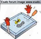
2. Since the LCD is made of glass, it may be damaged if it is bent. If it falls from a high place or receives a strong shock, the glass may be broken.
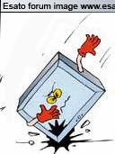
3. The LCD product is composed of sensitive electronic parts and components. Therefore it must be grounded by ESD protection equipment (wrist band, etc.) before it is directly handled.
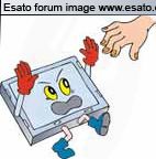
4. It is recommended that the product be handled with soft gloves during Assembly, etc. The LCD surface is made of soft film, vulnerable to scratches and thus to damage by a sharp articles.

5. Do not bend or stretch the back light wire.
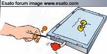
6. It is recommended that the product surface be cleaned it is dirty by using IPA (Isoprophyl Alcohol) or Hexane. Keytone type material (Acetone), Ethyl or Methyl chloride must not be used as they can cause damage to the Polarizer.
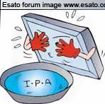
7. The Driver IC of the TFT LCD for a Notebook PC is exposed on the back of the screen. If mechanical stress is applied to this area, it can cause failure. Do not hold or press this part with your hands.

Usage
As LCD is a sensitive electronic equipment, it is urged to comply with following precautions.
1. Never disassemble LCD product under any circumstances. If unqualified operators or users assemble the product after disassembling it, it may not function or its operation may be seriously affected.

2 . When it is not in use, the screen must be turned off or the pattern must be frequently changed by a screen saver. If it displays the same pattern for a long period of time, brightness down/image sticking may develop due to the LCD structure.
3. It is recommended that the product be stored in a cool and dry place in its original product box.
4. Please dispose of the product according to the relevant laws and regulations. A small quantity of mercury is contained in lamp inside LCD product.

*Thanks and we would like to express our appreciation to Samsung Electronics for the preceding information.
Display Drivers Settings Customization TFT-LCD
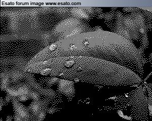
Color depth or bit depth, is a computer graphics term describing the number of bits used to represent the color of a single pixel in a bitmapped image or video frame buffer. This concept is also known as bits per pixel (bpp), particularly when specified along with the number of bits used. Higher color depth gives a broader range of distinct colors.
With relatively low color depth, the stored value is typically a number representing the index into a color map or palette. The colors available in the palette itself may be fixed by the hardware or modifiable within the limits of the hardware (for instance, both color Macintosh systems and VGA-equipped IBM-PCs typically ran at 8-bit due to limited VRAM, but while the best VGA systems only offered an 18-bit (262,144 color) palette from which colors could be chosen, all color Macintosh video hardware offered a 24-bit (16 million color) palette). Modifiable palettes are sometimes referred to as pseudocolor palettes.
1bit
4bit
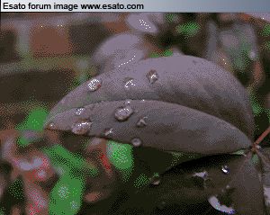
8bit

* 1-bit color (21 = 2 colors) monochrome, often black and white.
* 2-bit color (2� = 4 colors) CGA, gray-scale early NeXTstation, color Macintoshes.
* 3-bit color (2� = 8 colors) many early home computers with TV out displays
4 bits
* 4-bit color (24 = 16 colors) as used by EGA and by the least common denominator VGA standard at higher resolution, color Macintoshes.
* 5-bit color (25 = 32 colors) Original Amiga chipset
* 6-bit color (26 = 64 colors) Original Amiga chipset
8 bits
* 8-bit color (28 = 256 colors) most early color Unix workstations, VGA at low resolution, Super VGA, AGA, color Macintoshes.
* 12-bit color (212 = 4096 colors) some Silicon Graphics systems, Color NeXTstation systems, and Amiga systems in HAM mode.
Old graphics chips, particularly those used in home computers and video game consoles, often feature an additional level of palette mapping in order to increase the maximum number of simultaneously displayed colors. For example, in the ZX Spectrum, the picture is stored in a two-color format, but these two colors can be separately defined for each rectangular block of 8x8 pixels.
Direct color
As the number of bits increases, the number of possible colors becomes impractically large for a color map. So in higher color depths, the color value typically directly encodes relative brightnesses of red, green, and blue to specify a color in the RGB color model.
8-bit direct color
A very limited but true direct color system, there are 3 bits (8 possible levels) for both the R and G components, and the two remaining bits in the byte pixel to the B component (four levels), enabling 256 (8 � 8 � 4) different colors. The normal human eye is less sensitive to the blue component than to the red or green, so it is assigned one bit less than the others. Used, amongst others, in the MSX2 system series of computers in the early to mid 1990s.
Do not confuse with an indexed color depth of 8bpp (although it can be simulated in such systems by selecting the adequate table).
12-bit direct color
In 12-bit direct color, there are 4 bits (16 possible levels) for each of the R, G, and B components, enabling 4,096 (16 � 16 � 16) different colors. This color depth is sometimes used in mobile devices with a color display, such as mobile telephones and other equipment.
HighColor
Highcolor or HiColor is considered sufficient to provide life-like colors, and is encoded using either 15 or 16 bits:
* 15-bit uses 5 bits to represent red, 5 for green, and 5 for blue. Since 25 is 32 there are 32 levels of each color which can therefore be combined to give a total of 32,768 (32 � 32 � 32) mixed colors.
* Many 16-bit color schemes uses 5 bits to represent red, 5 bits to represent blue, but (since the human eye is more sensitive to the color green) uses 6 bits to represent 64 levels of green, sometimes known as 5650 format. These can therefore be combined to give 65,536 (32 � 64 � 32) mixed colors. Some formats like the Macintosh 16-bit color scheme known as "Thousands of colors" use 5 bits for each of the colors, and then the last bit for a 1-bit alpha value. There is another format that uses 4 bits for all colors and alpha, known as 4444 format.
LCD displays
* Some cheaper LCD displays use dithered 18-bit color (64 � 64 � 64 = 262,144 combinations) to achieve faster transition times, without sacrificing truecolor display levels entirely.
Truecolor
Truecolor (24+ bits)

Truecolor can mimic far more of the colors found in the real world, producing over 16.7 million distinct colors. This approaches the level at which megapixel monitors can display distinct colors for most photographic images, though image manipulation, monochromatic images (which are restricted to 256 levels, owing to their single channel), large images or �pure� generated images reveal banding and dithering artifacts.
* 24-bit truecolor uses 8 bits to represent red, 8 bits to represent blue and 8 bits to represent green. 28 = 256 levels of each of these three colors can therefore be combined to give a total of 16,777,216 mixed colors (256 � 256 � 256). Twenty-four-bit color is referred to as "millions of colors" on Macintosh systems.
30-bit color
Video cards with 10 bits per color, or 30-bit color, started coming into the market in the late 1990s. An early example was the Radius ThunderPower card for the Macintosh, which included extensions for Quickdraw and Photoshop plugins to support editing 30-bit images.
32-bit color
"32-bit color" is generally a misnomer in regard to display color depth. While actual 32-bit color at ten to eleven bits per channel produces over 4.2 billion distinct colors, the term �32-bit color� is most often a misuse referring to 24-bit color images with an additional eight bits of non-color data (I.E.: alpha, Z or bump data), or sometimes even to plain 24-bit data.
Systems using more than 24 bits in a 32-bit pixel for actual color data exist, but most of them opt for a 30-bit implementation with two bits of padding so that they can have an even 10 bits of color for each channel, similar to many HiColor systems.
Beyond truecolor
While some high-end graphics workstation systems and the accessories marketed toward use with such systems, as from SGI, have always used more than 8 bits per channel, such as 12 or 16 (36-bit or 48-bit color), such color depths have only worked their way into the general market more recently.
While practically every consumer brand of printer, scanner and digital camera on the market since the late 1990s offers 10, 12 or 16-bit DACs/ADCs, the ability to edit or see these colors onscreen has not seeped into modern PC systems. On the software front, working with high color depths in native RAW files is very difficult under Mac OS X, Microsoft Windows and most PC-based UNIX-likes, and many programs such as Photoshop or Final Cut are generally incapable of performing all operations �clean� for higher bit depths. On the hardware front, no consumer video adapter chipset has DACs better than 8-bit, and the integrated DACs in newer digital (LCD, PDP, etc�) monitors are often only 6-bit or worse.
As bit depths climb above twenty four, some systems are using the extra room to store data nonlinearly, with the most common form being the storage of more data than can be displayed all at once, as in extended dynamic range imaging, including high dynamic range imaging (HDRI). Floating point numbers are used to describe numbers in excess of 'full' white and black. This allows an image to describe accurately the intensity of the sun and deep shadows in the same color space for less distortion after intensive editing. Various models describe these ranges, many employing 32 bit accuracy per channel. A new format is the ILM "half" using 16-bit floating point numbers, it appears this is a much better use of 16 bits than using 16-bit integers and is likely to replace it entirely as hardware becomes fast enough to support it.
The ATI FireGL V7350 graphics card supports 40-bit and 64-bit color.
Television color
Most of today's TVs and computer screens form images by varying the intensity of just three primary colors: red, green, and blue. Bright yellow, for example, is composed of equal parts red and green, with no blue component. However, this is only an approximation, and is not as saturated as actual yellow light. For this reason, recent technologies such as Texas Instruments's BrilliantColor augment the typical red, green, and blue channels with up to three others: cyan, magenta and yellow.[3] Mitsubishi and Samsung, among others, use this technology in some TV sets. Assuming that 8 bits are used per color, such six-color images would have a color depth of 48 bits.
more info:
http://en.wikipedia.org
Display Drivers Settings Customization TFT-LCD based Sony, Hitachi, Epson...
INITIAL SEQUENCE DISPLAY
cap_resx=[#] # horizontal pixel resolution;=>default [f0]=240
cap_resy=[#] # vertical pixel resolution;=>default [140]=320
cap_bpp=[#] # bits per pixel;=>default [10] 16bit color addition
cap_bpp_high=[#] # bits per pixel;=>default [12] 18bit color addition
cap_bpppd=[#] # changed from 4;=>default [03]
cap_noofpd=[#] # changed from 2;=>default [01]
cap_freepdvert=[1] # added command, means pd mode can be placed in an arbitrary position;
pd_rectangle=; # predefined positions removed;
cap_width=[7788] # display width in micrometers;
cap_height=[9f60] # display height in micrometers;
cap_offset=[00 00]
cap_bigendian=[1]
cap_no_scanline_update=[1]
cap_update_x=[00 00]
INITIATION (START DISPLAY AFTER PHONE ON)
NORMAL TO SLEEP AND BACK
Properties:
#%d Percedes data that is considered to be a command string
#%w specifies a wait time in milliseconds
EMP PDI CODE
Properties:
pdipgmgcspeed=[#]=> Response Time
pdipgmwritespeed=[#]=> Response Time
pdipgmreadspeed=[#]=> Response Time
INITIAL SEQUENCE (GAMMA CURVE SETTINGS)
$00 08$ [##] [##]=>default [08]
init_seq=%d 00 d0 01;
init=%d $00 00 00 00 00 A4$ 00 01 %w1 %d
$00 08$ 08 08
$00 30$ 05 05
$00 31$ 05 05
$00 32$ 02 05
$00 33$ 03 00
$00 34$ 02 01
$00 35$ 01 03
$00 36$ 02 1A
$00 37$ 05 03
$00 38$ 05 05
$00 39$ 01 04
$00 3A$ 03 00
$00 3B$ 02 01
$00 3C$ 00 00
$00 3D$ 00 1F
$00 60$ 27 00
$00 61$ 00 00
$00 6A$ 00 00
$00 50$ 00 00
$00 51$ 00 EF
$00 52$ 00 00
$00 53$ 01 3F
$00 80$ 00 00
$00 81$ 00 00
$00 82$ 00 5F
$00 93$ 01 01
$00 07$ 00 00
$00 17$ 00 01
$00 19$ 00 00
$00 10$ 17 90
$00 11$ 00 07
$00 12$ 01 1D
$00 13$ 12 00
$00 12$ 01 3D
$00 01$ 01 00
$00 02$ 04 00
$00 03$ 12 30
$00 09$ 00 01
$00 0A$ 00 08
$00 0D$ 00 08 %wC8;
init2= %d $00 07$ 00 21 %w3C %d $00 10$ 16 90 $00 07$ 00 61 %w32 %d $00 07$ 01 73 %w15;
swreset=%d $00 00$ %w2 %d $00 00$ %w2 %d $00 00$ %w2 %d $00 00 00 00 00 00 00 00$;
all values are HEXADECIMAL
use calculator in scientific mode to convert dec hex
[ This Message was edited by: brazzuka's on 2009-12-10 15:29 ] |
brazzuka's
Joined: Nov 14, 2007
Posts: > 500
From: South World-Antartida-Sweden
PM, WWW
|
Sony Ericsson Display Drivers
Download
Display Drivers DB2010/DB2012 Phones
Sony Ericsson J300, D750, K300, K310, K320, K500, K510, K530, K600, K700, K750, S700, W200, W300, W550, W600, W700, W800, W810, Z520, Z525, Z530, Z550, Z558
Display Drivers Original:
-> Sony Ericsson k300/k310/k320 -> Download
-> Sony Ericsson z520 -> Download
-> Sony Ericsson z530 -> Download
-> Sony Ericsson z550 -> Download
-> Sony Ericsson k500/k510 -> Download
-> Sony Ericsson k600 -> Download
-> Sony Ericsson w550/w600 -> Download
-> Sony Ericsson d750 -> Download
-> Sony Ericsson w800/w810 -> Download
-> Sony Ericsson k750 -> Download
-> Sony Ericsson w200 -> Download
-> Sony Ericsson w300 -> Download
Display Drivers DB2020/DB2030 Phones
Sony Ericsson K530, K550, K550im, K610, K610im, K618, K660, K770, K790, K800, K810, K818, V630, S500, T650, T658, W580, W610, W660, W710, W830, W850, W880, Z555, Z610, Z710
Display Drivers Original:
-> Sony Ericsson k530 -> Download
-> Sony Ericsson w610/k550 -> Download
-> Sony Ericsson k610 -> Download
-> Sony Ericsson k790/k800/k810 -> Download
-> Sony Ericsson w580/s500 -> Download
-> Sony Ericsson w880 -> Download
Display Drivers DB3150(A2) Phones
Sony Ericsson C702, C902, K630, K660, K850, K858, T700, TM506, V640, W595 , W760, W902 , W908 , W890, W910, W980, Z750, Z770, Z780
Display Drivers Original:
-> Sony Ericsson c702 -> Download
-> Sony Ericsson c902 -> Download
-> Sony Ericsson k660 ->Download
-> Sony Ericsson k850 -> Download
-> Sony Ericsson t700 ->Download
-> Sony Ericsson tm506 ->Download
-> Sony Ericsson w595 -> Download
-> Sony Ericsson w760 -> Download
-> Sony Ericsson w890 ->Download
-> Sony Ericsson w910 -> Download
-> Sony Ericsson w980 -> Download
-> Sony Ericsson w902 -> Download
-> Sony Ericsson z750 ->Download
-> Sony Ericsson z780 ->Download
Display Drivers DB3210(A2) Phones
Sony Ericsson C510, C901, C903, C905, G705, T715, W705, W715, W995
Display Drivers Original:
-> Sony Ericsson c510 ->Download
-> Sony Ericsson c901 ->Download
-> Sony Ericsson c903 ->Download
-> Sony Ericsson c905 -> Download
-> Sony Ericsson g705 ->Download
-> Sony Ericsson t715 ->Download
-> Sony Ericsson w705 ->Download
-> Sony Ericsson w715 ->Download
-> Sony Ericsson w995 ->Download
Display Drivers DB3200(A2) Phones
Sony Ericsson F100-Jalou, J105-Naite, T707, W508
-> Sony Ericsson f100-Jalou ->
-> Sony Ericsson j105-Naite ->
-> Sony Ericsson t707 ->
-> Sony Ericsson w508 ->
Display Drivers DB3350(A2) Phones
Sony Ericsson U10-Aino, U100-Yari
-> Sony Ericsson U10-Aino ->
-> Sony Ericsson U100-Yari ->
Display Drivers DBpnx5230 Phones
Sony Ericsson w350, w380, t280, Z310, z555
Display Drivers Original:
-> Sony Ericsson w350/w380 -> Download
-> Sony Ericsson z310 -> Download
-> Sony Ericsson z555 -> Download
Display Drivers DBHB109 Phones
Sony Ericsson U1-Satio
Display Drivers PDA/Smartphones
Sony Ericsson G700, G900, M600, M608, P1, P990, W950, W960
Display Drivers Original:
Display Drivers PDA/Smartphones
Sony Ericsson Xperia X1
Display Drivers Original:
Display Drivers DBLocosto OEM platforms
J110, J120, J210, J220, J230, K205, K200, K220, T250, T258, T270, T280, T303, R300, R306, Z250, Z300, Z320
Display Drivers Original:
Sony Ericsson Developer Display Drivers
Here you can find developer or modding display drivers sony ericsson
Download
* not all phone models are supported
[ This Message was edited by: brazzuka's on 2009-12-10 12:11 ] |
ziupo
Joined: Apr 14, 2007
Posts: 74
PM |
And some modified versions DB3150?
I know that add dispdriver for K850i.
|
londa88
Joined: Oct 13, 2008
Posts: 10
From: Netherlands
PM |
are you making new display driver? |
@l+3r 3g0
Joined: Mar 27, 2008
Posts: 36
PM |
i got a question to ask. recently, i sent my k810 to a service centre to replace my LCD which went blue and white but no image. after i recieved my phone, it seems to me that the color of my LCD becomes somewhat pale. was it caused by the driver or the LCD itself? because the service centre updated my firmware too. |
serge327
Joined: Jun 06, 2008
Posts: 98
PM |
halo^^
can make a display driver for k800i?
i want the LCD display with more saturation...
because my new k800 screen dint same with old k800i LCD...
my new k800i screen with less suturation but smooth but, my old k800i LCD with more saturation....
#sorry for my bad english |
Navar
Joined: May 02, 2008
Posts: > 500
From: Jordan
PM |
Hi guys  i have a qustion..what the disdriver change?what it do to the screen?is it give much color or clean or what?and is it save? i have a qustion..what the disdriver change?what it do to the screen?is it give much color or clean or what?and is it save? |
Kanzleramt
Joined: Jun 14, 2008
Posts: 5
PM, WWW
|
this work for my k850 ? |
dantc702
Joined: Feb 20, 2009
Posts: 68
From: PH
PM |
is this applicable for c702?
"A simple guy just like as easy as eating TORON" -------------- * dant * |
Junz
Joined: Jul 31, 2008
Posts: > 500
From: INA
PM |
may be yes 
you can try it yourself but b4 doing that back up your original disp.driv |
dantc702
Joined: Feb 20, 2009
Posts: 68
From: PH
PM |
hmmm!!!! well, thats the safest way, to always have a back up. ill try to flash this to my phone and reflash to another one if it will not work. hope it will..
"A simple guy just like as easy as eating TORON" -------------- * dant * |
idumbakumar
Joined: Oct 01, 2007
Posts: > 500
From: chennai,india.
PM |
when i use ur modded display driver the camera refuses to save the pics.. please edit ur driver and let us know
i used this Display Driver BrAzzUkA's_v200902155 _for_w995.zip
and the main problem i faced is blue color and white
white is not clear sort of yellowish and the blue hue is less. it needs some more saturation so that the white become pure..
please will edit the driver for us
i created a topic here
hope u solve my problem....
|
mallaccra
Joined: Oct 01, 2007
Posts: > 500
PM |
-> Sony Ericsson w910 -> Download
The above link is not working...any other working link??
mallaccra®  Xperia Z2 |D6503|4.4.2|  Xperia Z1 |C6903|4.4.2|  Xperia Z |C6603|4.2.2|  Xperia ZL |C6502|4.2.2|  Xperia TX |LT29i|4.1.2|  Xperia Ion |LT28h|4.0.4|  Xperia P |LT22i|4.1.2|  Xperia J |ST26i|4.1.2|  Aino |
brazzuka's
Joined: Nov 14, 2007
Posts: > 500
From: South World-Antartida-Sweden
PM, WWW
|
@serge327
halo^^
can make a display driver for k800i?
i want the LCD display with more saturation...
because my new k800 screen dint same with old k800i LCD...
my new k800i screen with less suturation but smooth but, my old k800i LCD with more saturation....
#sorry for my bad english
try this look here:
http://www.esato.com/board/viewtopic.php?topic=157027
http://www.esato.com/board/viewtopic.php?topic=166030
@Navar
Hi guys i have a qustion..what the disdriver change?what it do to the screen?is it give much color or clean or what?and is it save?
basically the changes are:
(GAMMA CURVE SETTINGS)
EMP PDI CODE
Properties:
pdipgmgcspeed=[#]=> Response Time
pdipgmwritespeed=[#]=> Response Time
pdipgmreadspeed=[#]=> Response Time
@dantc702
is this applicable for c702?
for c702 yes
@idumbakumar
when i use ur modded display driver the camera refuses to save the pics.. please edit ur driver and let us know
i used this Display Driver BrAzzUkA's_v200902155 _for_w995.zip
and the main problem i faced is blue color and white
white is not clear sort of yellowish and the blue hue is less. it needs some more saturation so that the white become pure..
please will edit the driver for us
i created a topic here
hope u solve my problem....
for colors saturation you will have more luck on other drivers , camdrivers are most recommended for this.
Display drivers only.
the changes in the display is only visible to these properties:
(GAMMA CURVE SETTINGS)
EMP PDI CODE
Properties:
pdipgmgcspeed=[#]=> Response Time
pdipgmwritespeed=[#]=> Response Time
pdipgmreadspeed=[#]=> Response Time
about display driver the camera refuses to save the pics: let's look at what is happening and when we have free time and tnks for help
sorry but it not a big deal for dispdriver,we not want to end with their hopes but there are no miracles in the display driver no miracles.
@mallaccra
-> Sony Ericsson w910 -> Download
The above link is not working...any other working link??
link fix
Thank you for letting us know
| |
|
Access the forum with a mobile phone via esato.mobi
|